How to Stack Two Computer Chips with Direct Connections
TSMC's patent describes a compact way to stack two computer chips directly on top of each other, using a special filling material to hold tiny electrical connections in place, often with the top chip being wider than the bottom.
Original patent title: “Structure and method for 3D IC package”
TSMC's patent describes a compact way to stack two computer chips directly on top of each other, using a special filling material to hold tiny electrical connections in place, often with the top chip being wider than the bottom. Granted to Taiwan Semiconductor Manufacturing Co TSMC in 2016 with 23 claims and 1 forward citation, and it is expected to expire in 2035.
Coverage
What does this patent actually cover?
The patent describes a way to build a compact chip package by stacking a "first die" (a semiconductor chip) and a "second die" directly. An "underfill" material is placed between these two chips, making physical contact with both (ClaimclaimA numbered sentence at the end of a patent that legally defines what the inventor owns. The most important section.Read more → 1). Inside this underfill, tiny "conductive elements" (like solder bumps or under-bump metallization) create electrical connections between the first and second dies (Claim 1, Claim 5). The first die also has "interconnection layers" on its back side, which connect to the conductive elements through "through-vias" that pass all the way through the first die's semiconductor material (Claim 1). This allows for a very dense, direct connection between stacked chips. For example, a smaller processor chip could be stacked directly on a wider memory chip, with the underfill and surrounding molding compounds providing mechanical support for the wider top chip (Claim 9).
The gap
What does this patent NOT cover?
- Chip packages where the electrical connections between stacked dies are not fully encapsulated within an underfill material (ClaimclaimA numbered sentence at the end of a patent that legally defines what the inventor owns. The most important section.Read more → 1).
- Stacking chips that rely on an intermediate "interposer" substrate to connect the dies, rather than direct die-to-die connections (ClaimclaimA numbered sentence at the end of a patent that legally defines what the inventor owns. The most important section.Read more → 14).
- Chip packages where the electrical connections from the lower die do not pass through "through-vias" to interconnection layers on the opposite side (ClaimclaimA numbered sentence at the end of a patent that legally defines what the inventor owns. The most important section.Read more → 1).
- Packages where the first and second dies are not physically in contact with the underfill (ClaimclaimA numbered sentence at the end of a patent that legally defines what the inventor owns. The most important section.Read more → 1).
- Chip stacking methods that do not use molding compounds to encapsulate the dies and underfill (ClaimclaimA numbered sentence at the end of a patent that legally defines what the inventor owns. The most important section.Read more → 2, Claim 8).
These exclusions are unique to PatentBrief — derived from the actual claim language, not patent-office boilerplate.
Key facts
What made this novel
The noveltynoveltyThe requirement that an invention be different from anything publicly known before its priority date.Read more → lies in directly coupling two dies with conductive elements fully encapsulated in an underfill, combined with through-vias in the lower die connecting to external layers, and often supporting an "overhang" structure where the top chip is wider, all without an interposer. This creates a very compact and mechanically robust 3D package.
The Patent Drawing
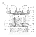
Schematic visualization of the patent's claim structure. Hand-drawn diagrams in progress for each landmark patent.
Where you've seen this
Real-world examples
High-bandwidth memory (HBM) stacks
Advanced smartphone processors with integrated memory
Graphics processing units (GPUs)
System-on-chip (SoC) packages
Multi-chip modules (MCMs)
Why it matters
The bigger picture
This patent is significant for creating high-density, compact electronic devices. By stacking chips directly and using underfill to secure connections, it enables more powerful functions in smaller spaces. This approach is crucial for advanced packaging technologies, allowing for better performance and lower power consumption in complex integrated circuits. TSMC, a leading chip manufacturer, uses such techniques to produce chips for a wide range of consumer electronics and high-performance computing.
Filed
March 20, 2015
Granted
August 9, 2016
Market context
Who's building on this
Companies in this space
Taiwan Semiconductor Manufacturing Company (TSMC), the assigneeassigneeThe entity that owns the patent — usually the inventor's employer or a company.Read more →, is a global leader in semiconductor manufacturing and continues to develop and utilize advanced 3D packaging technologies. Other major chip manufacturers and foundries, such as Samsung and Intel, are also actively developing and implementing similar advanced packaging solutions to create more compact and powerful integrated circuits. These techniques are critical for high-performance computing, AI accelerators, and mobile processors.
Market impact
This type of advanced packaging has significantly impacted the semiconductor market by enabling higher integration density and improved performance for complex chips. It allows for the creation of smaller, more powerful devices, driving innovation in areas like smartphones, data centers, and AI hardware. The ability to stack different types of chips, such as logic and memory, directly contributes to the development of System-on-Chip (SoC) designs and high-bandwidth memory, which are crucial components in today's technology landscape.
Claim 1 — Plain English
What this patent covers
The patent describes a way to build a compact chip package by stacking a "first die" (a semiconductor chip) and a "second die" directly. An "underfill" material is placed between these two chips, making physical contact with both (Claim 1). Inside this underfill, tiny "conductive elements" (like solder bumps or under-bump metallization) create electrical connections between the first and second dies (Claim 1, Claim 5). The first die also has "interconnection layers" on its back side, which connect to the conductive elements through "through-vias" that pass all the way through the first die's semiconductor material (Claim 1). This allows for a very dense, direct connection between stacked chips. For example, a smaller processor chip could be stacked directly on a wider memory chip, with the underfill and surrounding molding compounds providing mechanical support for the wider top chip (Claim 9).
The clever bit
The novelty lies in directly coupling two dies with conductive elements fully encapsulated in an underfill, combined with through-vias in the lower die connecting to external layers, and often supporting an "overhang" structure where the top chip is wider, all without an interposer. This creates a very compact and mechanically robust 3D package.
What it does not cover
- Chip packages where the electrical connections between stacked dies are not fully encapsulated within an underfill material (Claim 1).
- Stacking chips that rely on an intermediate "interposer" substrate to connect the dies, rather than direct die-to-die connections (Claim 14).
- Chip packages where the electrical connections from the lower die do not pass through "through-vias" to interconnection layers on the opposite side (Claim 1).
- Packages where the first and second dies are not physically in contact with the underfill (Claim 1).
- Chip stacking methods that do not use molding compounds to encapsulate the dies and underfill (Claim 2, Claim 8).
Patent timeline
Application submitted to the patent office
Application published, typically 18 months after filing
Patent officially issued
Patent enters public domain
PatentBrief Score
Impact Score
Early stage
Citation count
6/40
Early citations
Claim breadth
15/20
Broad claimsclaimsThe numbered statements at the end of a patent that legally define what the inventor owns.Read more →
Recency
5/20
Granted 10–20 years ago
Assignee scale
0/20
Independent or smaller assigneeassigneeThe entity that owns the patent — usually the inventor's employer or a company.Read more →
PatentBrief Impact Score — based on citation count, claim breadth, recency, and assignee scale. Not a legal assessment.
Heuristic Value Estimate
What this patent might be worth
$59K – $187K
Midpoint $117K · 8.5 yr remaining · industry ×1.5
Heuristic only — blends forward/backward citation counts, claim scope, time remaining, litigation history, and CPC-derived industry baseline. Real valuations need a professional appraisal.
Claim text not yet imported for this patent
The original legal language
Original claims
23 claims as filed with the patent office.
Concepts involved
Citations
Patent lineage
Cite this patent
Yu, C., Yeh, D., Jeng, S., & Hou, S. (2016). How to Stack Two Computer Chips with Direct Connections (U.S. Patent No. 9,412,678). U.S. Patent and Trademark Office. https://patentbrief.org/patent/us/9412678/structure-and-method-for-3d-ic-package
Auto-generated from the patent record. Double-check author order and the issue date against the official USPTO document before submitting.
Embed
Add this patent to your site
Drop this plain-English patent card into any blog post or article — free, no signup. It always links back to the full breakdown here.
<div data-patentlens-widget data-patent-number="US9412678"></div>
<script src="https://patentbrief.org/embed.js" async></script>
Stay in the loop
Get a weekly digest of new patents.
One email per week. No spam. Unsubscribe anytime.
Keep exploring
Related patents you should know
US 4683195 · 1987
How to Make Billions of Copies of a DNA Segment
This patent describes the Polymerase Chain Reaction (PCR), a method to rapidly create many copies of a specific piece of DNA or RNA, enabling its detection and analysis.
Cetus Corp
US 8697359 · 2014
How to Edit Genes in Human Cells Using an Engineered CRISPR System
This patent describes an engineered CRISPR-Cas9 system for precisely cutting DNA in eukaryotic cells to change how genes work, opening the door for gene editing in complex organisms.
Massachusetts Institute of Technology
US 7657849 · 2010
How the iPhone's Slide-to-Unlock Gesture Works
Apple's 2010 patent describes unlocking a device by dragging a specific graphical image across the touchscreen along a predefined path, a gesture that became iconic with the original iPhone.
Apple Inc
US 4733665 · 1988
How Doctors Implant a Permanent Stent Using a Balloon
This patent describes the method for placing a permanent, expandable wire mesh tube inside a blood vessel or other body tube using a balloon-tipped catheter to widen it and keep it open.
Expandable Grafts Partnership
US 4965188 · 1990
How to Make Many Copies of a DNA Piece with Heat
This patent describes the Polymerase Chain Reaction (PCR) method, a technique to make millions of copies of a specific DNA segment using a heat-resistant enzyme and repeated temperature changes.
Cetus Corp
US 4235871 · 1980
How to Encapsulate Active Materials in Lipid Bubbles Efficiently
This patent describes a method for trapping biologically active substances inside tiny, multi-layered fat bubbles called liposomes, using a specific water-in-oil emulsion and gel-forming process to improve how much material gets captured.
Individual
Semantically similar
You might also find these interesting
US 7824959 · 2010 · Samsung Electronics Co
How to Stack Computer Chips on a Wafer for Smaller Devices
US 8310051 · 2012 · MediaTek
How Chips Are Stacked and Wired in Tiny Phone Parts
US 12181722 · 2024 · Taiwan Semiconductor Manufacturing Co TSMC
Stacking Chips with Light-Guiding Plastic Wires
US 12326604 · 2025 · Corning
How Chips Get Both Light and Electricity on a Special Glass Base
More to explore
More in Semiconductors & Chips
US 5563422 · 1996 · Nichia Chemical Industries Ltd
How Nichia Created the First Practical Blue LED Electrodes
US 10373050 · 2019 · Qualcomm Inc
How to Make AI Run Faster on Smaller Computer Chips
US 2981877 · 1961 · Fairchild Semiconductor Corp
How Robert Noyce Invented the Modern Integrated Circuit
US 2569347 · 1951 · Bell Telephone Laboratories Inc
The Invention of the Junction Transistor
New to patents?
Common Questions
Frequently Asked Questions
What does How to Stack Two Computer Chips with Direct Connections cover?
TSMC's patent describes a compact way to stack two computer chips directly on top of each other, using a special filling material to hold tiny electrical connections in place, often with the top chip being wider than the bottom.
Who owns patent US 9412678?
Taiwan Semiconductor Manufacturing Co TSMC owns this patent, granted in 2016.
When does this patent expire?
This patent is expected to expire on March 20, 2035, when the invention enters the public domain.
What is patent US 9412678 cited by?
This patent has been cited by 1 later patents that build on its ideas.
What problem does this patent solve?
This patent is significant for creating high-density, compact electronic devices. By stacking chips directly and using underfill to secure connections, it enables more powerful functions in smaller spaces. This approach is crucial for advanced packaging technologies, allowing for better performance and lower power consumption in complex integrated circuits. TSMC, a leading chip manufacturer, uses such techniques to produce chips for a wide range of consumer electronics and high-performance computing.
What does this patent NOT cover?
Chip packages where the electrical connections between stacked dies are not fully encapsulated within an underfill material (Claim 1).
Same assignee
More from Taiwan Semiconductor Manufacturing Co TSMC
Patent monitoring