How to Embed Tiny Optical Components Directly into Circuit Boards
A design for embedding light-emitting components and light-guiding paths directly into the layers of a circuit board to make devices smaller and more efficient.
Original patent title: “USRE50510E1 - Optical device”
A design for embedding light-emitting components and light-guiding paths directly into the layers of a circuit board to make devices smaller and more efficient. Granted to Sony Group Corp in 2025 with 62 claims.
Coverage
What does this patent actually cover?
This patent describes a way to carve a hole, or recessed part, into a multilayer circuit board to create a home for optical parts like lasers or sensors. By cutting through the top insulating layers to reach internal wiring patterns, the design allows the optical element to sit flush within the board itself. An optical waveguide—a tiny pipe for light—is also placed in this hole to direct light along the surface of the board. This setup creates a direct, compact connection between the electrical circuits and the optical components, which is useful for high-speed data transmission or sensing.
The gap
What does this patent NOT cover?
- Does not cover optical devices that sit on top of a circuit board without being recessed into the layers.
- Does not cover standard fiber optic cables that are not integrated into the board's recessed structure.
- Does not cover light-emitting components that lack an electrical connection to the internal wiring patterns of the multilayer substrate.
These exclusions are unique to PatentBrief — derived from the actual claim language, not patent-office boilerplate.
Key facts
What made this novel
The innovation is using the circuit board's own internal wiring layers as the mounting and electrical interface for the optical component, effectively turning the board into a structural housing for the light path.
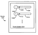
Schematic visualization of the patent's claim structure. Hand-drawn diagrams in progress for each landmark patent.
Where you've seen this
Real-world examples
High-speed optical transceivers
Compact laser-based sensors for mobile devices
Integrated photonic circuit boards
Why it matters
The bigger picture
As electronics shrink, the bottleneck often becomes how to move data quickly between chips. By integrating light-based components directly into the circuit board, companies like Sony can reduce the physical space required for optical communication, potentially leading to faster and more compact hardware for data centers or mobile devices.
Filed
April 26, 2021
Granted
July 29, 2025
Market context
Who's building on this
Companies in this space
Sony Group Corp is the primary assigneeassigneeThe entity that owns the patent — usually the inventor's employer or a company.Read more →. The technology is relevant to major semiconductor and telecommunications companies like Intel, Broadcom, or NVIDIA, who are actively working on silicon photonics to replace traditional copper wiring for data movement.
Market impact
This patent supports the industry shift toward silicon photonics, where light is used instead of electricity to move data across circuit boards. By standardizing how these components are physically integrated, it helps manufacturers move away from bulky, separate optical modules toward fully integrated, board-level optical systems.
Claim 1 — Plain English
What this patent covers
This patent describes a way to carve a hole, or recessed part, into a multilayer circuit board to create a home for optical parts like lasers or sensors. By cutting through the top insulating layers to reach internal wiring patterns, the design allows the optical element to sit flush within the board itself. An optical waveguide—a tiny pipe for light—is also placed in this hole to direct light along the surface of the board. This setup creates a direct, compact connection between the electrical circuits and the optical components, which is useful for high-speed data transmission or sensing.
The clever bit
The innovation is using the circuit board's own internal wiring layers as the mounting and electrical interface for the optical component, effectively turning the board into a structural housing for the light path.
What it does not cover
- Does not cover optical devices that sit on top of a circuit board without being recessed into the layers.
- Does not cover standard fiber optic cables that are not integrated into the board's recessed structure.
- Does not cover light-emitting components that lack an electrical connection to the internal wiring patterns of the multilayer substrate.
Patent timeline
Application submitted to the patent office
Application published, typically 18 months after filing
Patent officially issued
PatentBrief Score
Impact Score
Strong
Citation count
0/40
No citations yet
Claim breadth
20/20
Very broad protection
Recency
20/20
Granted within 5 years
Assignee scale
20/20
Major company or institution
PatentBrief Impact Score — based on citation count, claim breadth, recency, and assignee scale. Not a legal assessment.
Heuristic Value Estimate
What this patent might be worth
$43K – $138K
Midpoint $86K · 14.7 yr remaining · industry ×1.5
Heuristic only — blends forward/backward citation counts, claim scope, time remaining, litigation history, and CPC-derived industry baseline. Real valuations need a professional appraisal.
Claim text not yet imported for this patent
The original legal language
Original claims
62 claims as filed with the patent office.
Concepts involved
Citations
Patent lineage
Cite this patent
Naruse, T., & Arakida, T. (2025). How to Embed Tiny Optical Components Directly into Circuit Boards (U.S. Patent No. RE50,510). U.S. Patent and Trademark Office. https://patentbrief.org/patent/us/RE50510/gemini-bard
Auto-generated from the patent record. Double-check author order and the issue date against the official USPTO document before submitting.
Embed
Add this patent to your site
Drop this plain-English patent card into any blog post or article — free, no signup. It always links back to the full breakdown here.
<div data-patentlens-widget data-patent-number="USRE50510"></div>
<script src="https://patentbrief.org/embed.js" async></script>
Stay in the loop
Get a weekly digest of new patents.
One email per week. No spam. Unsubscribe anytime.
Keep exploring
Related patents you should know
US 4683195 · 1987
How to Make Billions of Copies of a DNA Segment
This patent describes the Polymerase Chain Reaction (PCR), a method to rapidly create many copies of a specific piece of DNA or RNA, enabling its detection and analysis.
Cetus Corp
US 8697359 · 2014
How to Edit Genes in Human Cells Using an Engineered CRISPR System
This patent describes an engineered CRISPR-Cas9 system for precisely cutting DNA in eukaryotic cells to change how genes work, opening the door for gene editing in complex organisms.
Massachusetts Institute of Technology
US 7657849 · 2010
How the iPhone's Slide-to-Unlock Gesture Works
Apple's 2010 patent describes unlocking a device by dragging a specific graphical image across the touchscreen along a predefined path, a gesture that became iconic with the original iPhone.
Apple Inc
US 4733665 · 1988
How Doctors Implant a Permanent Stent Using a Balloon
This patent describes the method for placing a permanent, expandable wire mesh tube inside a blood vessel or other body tube using a balloon-tipped catheter to widen it and keep it open.
Expandable Grafts Partnership
US 4965188 · 1990
How to Make Many Copies of a DNA Piece with Heat
This patent describes the Polymerase Chain Reaction (PCR) method, a technique to make millions of copies of a specific DNA segment using a heat-resistant enzyme and repeated temperature changes.
Cetus Corp
US 4235871 · 1980
How to Encapsulate Active Materials in Lipid Bubbles Efficiently
This patent describes a method for trapping biologically active substances inside tiny, multi-layered fat bubbles called liposomes, using a specific water-in-oil emulsion and gel-forming process to improve how much material gets captured.
Individual
Semantically similar
You might also find these interesting

US 12326604 · 2025 · Corning
How Chips Get Both Light and Electricity on a Special Glass Base

US 9055681 · 2015 · International Business Machines
Attaching Flexible Circuits with Light Sensors to a Chip

US 12181722 · 2024 · Taiwan Semiconductor Manufacturing Co TSMC
Stacking Chips with Light-Guiding Plastic Wires
US 12310123 · 2025 · Taiwan Semiconductor Manufacturing Co TSMC Ltd
How TSMC Makes Advanced Silicon-Based Light Sensors
More to explore
More in Consumer Electronics
US 7657849 · 2010 · Apple Inc
How the iPhone's Slide-to-Unlock Gesture Works
US 7479949 · 2009 · Apple Inc
How Touchscreens Understand Your Finger Swipes and Scrolls
US 4528643 · 1985 · FPDC Inc
How Stores Make Custom Products On-Demand with Remote Approval
US 7469381 · 2008 · Apple Inc
How Touchscreens Show and Snap Back When You Scroll Past an Edge
New to patents?
Common Questions
Frequently Asked Questions
What does How to Embed Tiny Optical Components Directly into Circuit Boards cover?
A design for embedding light-emitting components and light-guiding paths directly into the layers of a circuit board to make devices smaller and more efficient.
Who owns patent US RE50510?
Sony Group Corp owns this patent, granted in 2025.
When does this patent expire?
This patent is expected to expire on July 29, 2045, when the invention enters the public domain.
What problem does this patent solve?
As electronics shrink, the bottleneck often becomes how to move data quickly between chips. By integrating light-based components directly into the circuit board, companies like Sony can reduce the physical space required for optical communication, potentially leading to faster and more compact hardware for data centers or mobile devices.
What does this patent NOT cover?
Does not cover optical devices that sit on top of a circuit board without being recessed into the layers.
Patent monitoring