How to Stop Transistors from Wearing Out in Radio Frequency Chips
A method for extending the lifespan of silicon-on-insulator transistors by using a special sink to drain away charge that causes gate oxide breakdown.
Original patent title: “USRE48965E1 - Method and apparatus improving gate oxide reliability by controlling accumulated charge”
A method for extending the lifespan of silicon-on-insulator transistors by using a special sink to drain away charge that causes gate oxide breakdown. Granted to PSemi Corp in 2022 with 110 claims.
Coverage
What does this patent actually cover?
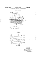
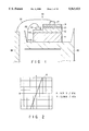
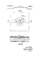
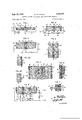
This patent describes a technique to prevent the premature failure of transistors used in radio frequency (RF) switches. When transistors are built on a silicon-on-insulator (SOI) substrate, they can accumulate unwanted electrical charge in their body, which stresses the thin gate oxide layer and leads to time-dependent dielectric breakdown (TDDB). The invention adds an 'accumulated charge sink' (ACS) to the transistor body. By applying a negative bias voltage to this sink, the system actively removes the accumulated charge, keeping the gate oxide healthy and extending the life of the device.
The gap
What does this patent NOT cover?
- Does not cover standard bulk silicon MOSFETs that do not use an SOI substrate.
- Does not cover charge control methods that rely solely on positive bias voltages.
- Does not cover transistors lacking a dedicated body contact or sink for charge removal.
These exclusions are unique to PatentBrief — derived from the actual claim language, not patent-office boilerplate.
Key facts
What made this novel
The innovation lies in recognizing that the 'body' of an SOI transistor is electrically floating, which allows charge to build up and degrade the oxide. By providing a controlled path to drain this charge using a negative bias, the inventors turned a parasitic effect into a manageable circuit parameter.
Schematic visualization of the patent's claim structure. Hand-drawn diagrams in progress for each landmark patent.
Where you've seen this
Real-world examples
RF front-end modules in 4G and 5G smartphones
High-performance antenna switches
SOI-based power amplifiers
Why it matters
The bigger picture
RF switches are essential components in modern smartphones and wireless hardware, allowing devices to toggle between different frequency bands. As these devices shrink, the gate oxide layers in transistors become thinner and more prone to failure. This technology is critical for ensuring that high-performance RF front-end modules remain reliable over the multi-year lifespan of a consumer device.
Filed
December 11, 2019
Granted
March 8, 2022
Market context
Who's building on this
Companies in this space
PSemi Corporation (formerly Peregrine Semiconductor) is the primary developer of this technology. Their SOI-based RF switch designs are foundational to the industry, and they continue to refine these charge control techniques for increasingly dense 5G radio frequency modules.
Market impact
This technology enabled the transition of RF switches from traditional silicon-on-sapphire to more cost-effective and scalable silicon-on-insulator processes. It effectively solved a major reliability bottleneck, allowing manufacturers to pack more switches into smaller spaces without sacrificing the longevity of the device.
Claim 1 — Plain English
What this patent covers
This patent describes a technique to prevent the premature failure of transistors used in radio frequency (RF) switches. When transistors are built on a silicon-on-insulator (SOI) substrate, they can accumulate unwanted electrical charge in their body, which stresses the thin gate oxide layer and leads to time-dependent dielectric breakdown (TDDB). The invention adds an 'accumulated charge sink' (ACS) to the transistor body. By applying a negative bias voltage to this sink, the system actively removes the accumulated charge, keeping the gate oxide healthy and extending the life of the device.
The clever bit
The innovation lies in recognizing that the 'body' of an SOI transistor is electrically floating, which allows charge to build up and degrade the oxide. By providing a controlled path to drain this charge using a negative bias, the inventors turned a parasitic effect into a manageable circuit parameter.
What it does not cover
- Does not cover standard bulk silicon MOSFETs that do not use an SOI substrate.
- Does not cover charge control methods that rely solely on positive bias voltages.
- Does not cover transistors lacking a dedicated body contact or sink for charge removal.
Patent timeline
Application submitted to the patent office
Application published, typically 18 months after filing
Patent officially issued
PatentBrief Score
Impact Score
Moderate
Citation count
0/40
No citations yet
Claim breadth
20/20
Very broad protection
Recency
20/20
Granted within 5 years
Assignee scale
0/20
Independent or smaller assigneeassigneeThe entity that owns the patent — usually the inventor's employer or a company.Read more →
PatentBrief Impact Score — based on citation count, claim breadth, recency, and assignee scale. Not a legal assessment.
Heuristic Value Estimate
What this patent might be worth
$50K – $161K
Midpoint $101K · 13.4 yr remaining · industry ×1.4
Heuristic only — blends forward/backward citation counts, claim scope, time remaining, litigation history, and CPC-derived industry baseline. Real valuations need a professional appraisal.
Claim text not yet imported for this patent
The original legal language
Original claims
110 claims as filed with the patent office.
Concepts involved
Citations
Patent lineage
Cite this patent
Kim, T. Y., Brindle, C. N., Stuber, M. A., Kelly, D. J., Imthurn, G. P., Dribinsky, A., Kemerling, C. L., Welstand, R. B., & Burgener, M. L. (2022). How to Stop Transistors from Wearing Out in Radio Frequency Chips (U.S. Patent No. RE48,965). U.S. Patent and Trademark Office. https://patentbrief.org/patent/us/RE48965/google-play-store
Auto-generated from the patent record. Double-check author order and the issue date against the official USPTO document before submitting.
Embed
Add this patent to your site
Drop this plain-English patent card into any blog post or article — free, no signup. It always links back to the full breakdown here.
<div data-patentlens-widget data-patent-number="USRE48965"></div>
<script src="https://patentbrief.org/embed.js" async></script>
Stay in the loop
Get a weekly digest of new patents.
One email per week. No spam. Unsubscribe anytime.
Keep exploring
Related patents you should know
US 4683195 · 1987
How to Make Billions of Copies of a DNA Segment
This patent describes the Polymerase Chain Reaction (PCR), a method to rapidly create many copies of a specific piece of DNA or RNA, enabling its detection and analysis.
Cetus Corp
US 8697359 · 2014
How to Edit Genes in Human Cells Using an Engineered CRISPR System
This patent describes an engineered CRISPR-Cas9 system for precisely cutting DNA in eukaryotic cells to change how genes work, opening the door for gene editing in complex organisms.
Massachusetts Institute of Technology
US 7657849 · 2010
How the iPhone's Slide-to-Unlock Gesture Works
Apple's 2010 patent describes unlocking a device by dragging a specific graphical image across the touchscreen along a predefined path, a gesture that became iconic with the original iPhone.
Apple Inc
US 4733665 · 1988
How Doctors Implant a Permanent Stent Using a Balloon
This patent describes the method for placing a permanent, expandable wire mesh tube inside a blood vessel or other body tube using a balloon-tipped catheter to widen it and keep it open.
Expandable Grafts Partnership
US 4965188 · 1990
How to Make Many Copies of a DNA Piece with Heat
This patent describes the Polymerase Chain Reaction (PCR) method, a technique to make millions of copies of a specific DNA segment using a heat-resistant enzyme and repeated temperature changes.
Cetus Corp
US 4235871 · 1980
How to Encapsulate Active Materials in Lipid Bubbles Efficiently
This patent describes a method for trapping biologically active substances inside tiny, multi-layered fat bubbles called liposomes, using a specific water-in-oil emulsion and gel-forming process to improve how much material gets captured.
Individual
Semantically similar
You might also find these interesting
US 12255678 · 2025 · Silicon Laboratories Inc
How Wireless Radios Automatically Adjust to Avoid Signal Overload
US RE49538 · 2023 · Samsung Electronics Co Ltd
How Samsung Makes Better Transistor Gates Using Two-Layer Metal Stacks
US 8831529 · 2014 · Apple Inc
How Smartphones Calibrate Their Radio Power Across Different Temperatures
US 3102230 · 1963 · Bell Telephone Laboratories Inc
The Invention of the Modern Field-Effect Transistor
More to explore
More in Semiconductors & Chips
US 5563422 · 1996 · Nichia Chemical Industries Ltd
How Nichia Created the First Practical Blue LED Electrodes
US 10373050 · 2019 · Qualcomm Inc
How to Make AI Run Faster on Smaller Computer Chips
US 2981877 · 1961 · Fairchild Semiconductor Corp
How Robert Noyce Invented the Modern Integrated Circuit
US 2569347 · 1951 · Bell Telephone Laboratories Inc
The Invention of the Junction Transistor
New to patents?
Common Questions
Frequently Asked Questions
What does How to Stop Transistors from Wearing Out in Radio Frequency Chips cover?
A method for extending the lifespan of silicon-on-insulator transistors by using a special sink to drain away charge that causes gate oxide breakdown.
Who owns patent US RE48965?
PSemi Corp owns this patent, granted in 2022.
When does this patent expire?
This patent is expected to expire on March 8, 2042, when the invention enters the public domain.
What problem does this patent solve?
RF switches are essential components in modern smartphones and wireless hardware, allowing devices to toggle between different frequency bands. As these devices shrink, the gate oxide layers in transistors become thinner and more prone to failure. This technology is critical for ensuring that high-performance RF front-end modules remain reliable over the multi-year lifespan of a consumer device.
What does this patent NOT cover?
Does not cover standard bulk silicon MOSFETs that do not use an SOI substrate.
Patent monitoring