Semiconductor lithography process
A semiconductor lithography process. A photoresist film is coated on a substrate. The photoresist film is subjected to a flood exposure to blanket expose the photoresist film across the substrate to a first radiation wit…
Original patent title: “Semiconductor lithography process”
A semiconductor lithography process. A photoresist film is coated on a substrate. The photoresist film is subjected to a flood exposure to blanket expose the photoresist film across the substrate to a first radiation wit…. Granted to Nanya Technology in 2012 with 18 claims and 3 forward citations, and it is expected to expire in 2030.
Coverage
What does this patent actually cover?
A semiconductor lithography process. A photoresist film is coated on a substrate. The photoresist film is subjected to a flood exposure to blanket expose the photoresist film across the substrate to a first radiation with a relatively lower dosage. The photoresist film is then subjected to a main exposure using a photomask to expose the photoresist film in a step and scan manner to a second radiation with a relatively higher dosage. After baking, the photoresist film is developed.
The gap
What does this patent NOT cover?
These exclusions are unique to PatentBrief — derived from the actual claim language, not patent-office boilerplate.
Key facts
The Patent Drawing
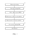
Schematic visualization of the patent's claim structure. Hand-drawn diagrams in progress for each landmark patent.
Patent Abstract
Patent abstract
A semiconductor lithography process. A photoresist film is coated on a substrate. The photoresist film is subjected to a flood exposure to blanket expose the photoresist film across the substrate to a first radiation with a relatively lower dosage. The photoresist film is then subjected to a main exposure using a photomask to expose the photoresist film in a step and scan manner to a second radiation with a relatively higher dosage. After baking, the photoresist film is developed.
Patent timeline
Application submitted to the patent office
Application published, typically 18 months after filing
Patent officially issued
Patent enters public domain
PatentBrief Score
Impact Score
Early stage
Citation count
12/40
Early citations
Claim breadth
12/20
Broad claimsclaimsThe numbered statements at the end of a patent that legally define what the inventor owns.Read more →
Recency
5/20
Granted 10–20 years ago
Assignee scale
0/20
Independent or smaller assigneeassigneeThe entity that owns the patent — usually the inventor's employer or a company.Read more →
PatentBrief Impact Score — based on citation count, claim breadth, recency, and assignee scale. Not a legal assessment.
Heuristic Value Estimate
What this patent might be worth
$34K – $109K
Midpoint $68K · 3.4 yr remaining · industry ×1.5
Heuristic only — blends forward/backward citation counts, claim scope, time remaining, litigation history, and CPC-derived industry baseline. Real valuations need a professional appraisal.
Claim text not yet imported for this patent
The original legal language
Original claims
18 claims as filed with the patent office.
Concepts involved
Citations
Patent lineage
Cite this patent
Huang, P., Wang, Y., & Huang, C. (2012). Semiconductor lithography process (U.S. Patent No. 8,124,319). U.S. Patent and Trademark Office. https://patentbrief.org/patent/us/8124319/semiconductor-lithography-process
Auto-generated from the patent record. Double-check author order and the issue date against the official USPTO document before submitting.
Embed
Add this patent to your site
Drop this plain-English patent card into any blog post or article — free, no signup. It always links back to the full breakdown here.
<div data-patentlens-widget data-patent-number="US8124319"></div>
<script src="https://patentbrief.org/embed.js" async></script>
Stay in the loop
Get a weekly digest of new patents.
One email per week. No spam. Unsubscribe anytime.
Keep exploring
Related patents you should know
US 4683195 · 1987
How to Make Billions of Copies of a DNA Segment
This patent describes the Polymerase Chain Reaction (PCR), a method to rapidly create many copies of a specific piece of DNA or RNA, enabling its detection and analysis.
Cetus Corp
US 8697359 · 2014
How to Edit Genes in Human Cells Using an Engineered CRISPR System
This patent describes an engineered CRISPR-Cas9 system for precisely cutting DNA in eukaryotic cells to change how genes work, opening the door for gene editing in complex organisms.
Massachusetts Institute of Technology
US 7657849 · 2010
How the iPhone's Slide-to-Unlock Gesture Works
Apple's 2010 patent describes unlocking a device by dragging a specific graphical image across the touchscreen along a predefined path, a gesture that became iconic with the original iPhone.
Apple Inc
US 4733665 · 1988
How Doctors Implant a Permanent Stent Using a Balloon
This patent describes the method for placing a permanent, expandable wire mesh tube inside a blood vessel or other body tube using a balloon-tipped catheter to widen it and keep it open.
Expandable Grafts Partnership
US 4965188 · 1990
How to Make Many Copies of a DNA Piece with Heat
This patent describes the Polymerase Chain Reaction (PCR) method, a technique to make millions of copies of a specific DNA segment using a heat-resistant enzyme and repeated temperature changes.
Cetus Corp
US 4235871 · 1980
How to Encapsulate Active Materials in Lipid Bubbles Efficiently
This patent describes a method for trapping biologically active substances inside tiny, multi-layered fat bubbles called liposomes, using a specific water-in-oil emulsion and gel-forming process to improve how much material gets captured.
Individual
New to patents?
Common Questions
Frequently Asked Questions
Who owns patent US 8124319?
Nanya Technology owns this patent, granted in 2012.
When does this patent expire?
This patent is expected to expire on April 12, 2030, when the invention enters the public domain.
What is patent US 8124319 cited by?
This patent has been cited by 3 later patents that build on its ideas.
Patent monitoring